


By Ralph Delmdahl, Rainer Pätzel, Rolf Senczuk and Jan Brune
Glass is a promising material from which advanced interposers for high density electrical interconnects for 2.5D and 3D chip packaging can be produced. The supply of ultra-thin glass wafers with thicknesses of 100 µm and below shows attractive cost and superior high frequency performance relative to polished thin wafers made of silicon. As thin glass is extremely brittle, micromachining to create through glass vias is particularly challenging and laser processing using deep UV excimer lasers at a wavelength of 193 nm and ultra-short pulse laser provide a viable solution.
The excimer laser has become a preferred technology in microelectronics manufacturing because it offers substantial advantages over alternative technologies. In particular, its non-contact nature and scalable output power enables the production of small, high precision features on a wide variety of materials. Frequently, it supports faster process throughput speeds and better yields with superior process consistency.
An excimer laser delivering high energy pulses of 600 mJ and having a pulse width of 25 ns was used as the laser source. Homogeneous square fields of equal laser fluence are projected with high demagnification onto the glass samples. An x-y-stage is used for moving the sample under the projection lens. For parallel through hole drilling at a wavelength of 193 nm, laser energy densities of more than 10 J/cm2 at the sample surface can be generated over field sizes of up to 1 mm2. In this work, we have used thin borosilicate glass wafers and alkali-free flat glass wafers of down to 30 µm thickness.
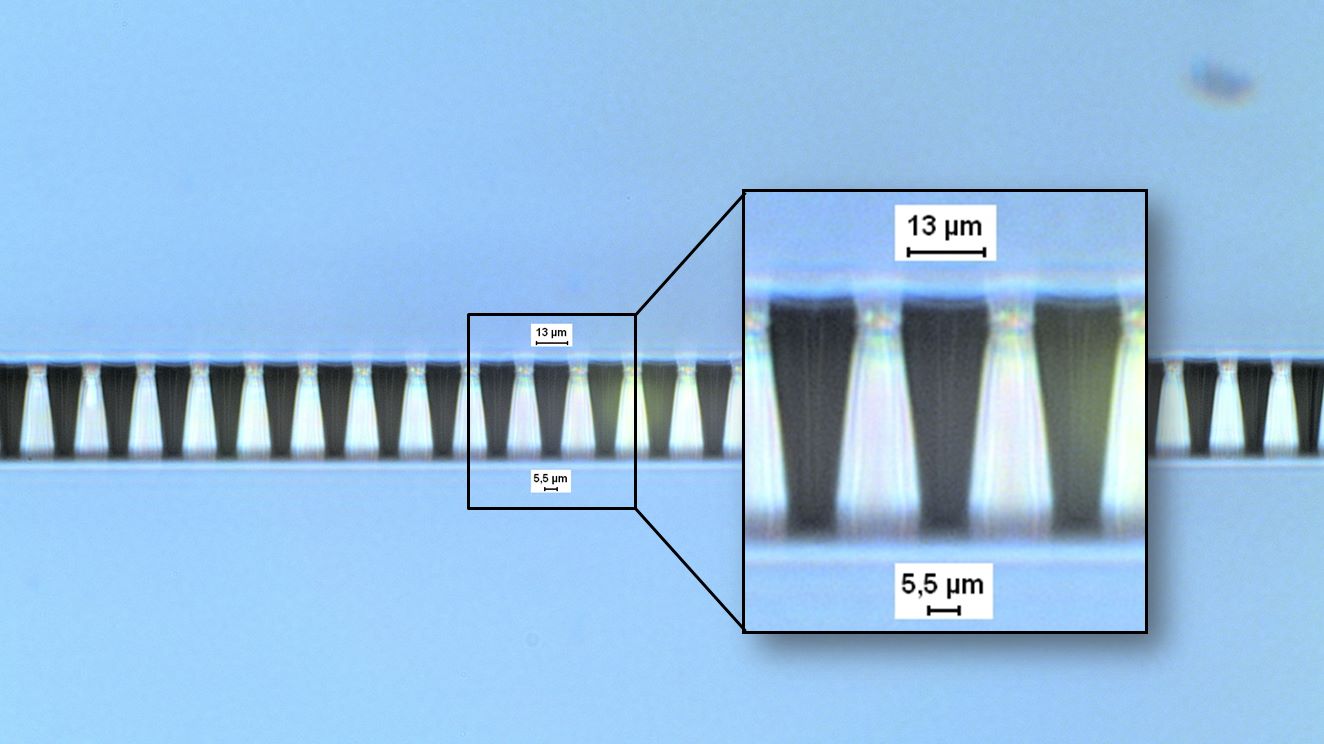
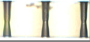
Through the experiments, it was found that mask projection drilling at a fluence of 7 J/cm2 provided the best combination of drilling speed and via hole quality. The obtained through holes are very symmetric and exhibit excellent pattern reproducibility. A double-side drilling approach can be applied for 100 µm glass wafer drilling which enables a strongly reduced taper angle.
Whereas in serial glass drilling the number of vias per time remains constant, the rate of parallel drilling as used in this work growths with the square of the pitch size. Consequently, a decreasing pitch size favors parallel drilling using excimer lasers.
The market trend to thinner glass wafers approaching the 30 µm mark and both smaller via and pitch dimensions, will accelerate the adoption of excimer lasers in high density through glass via drilling.
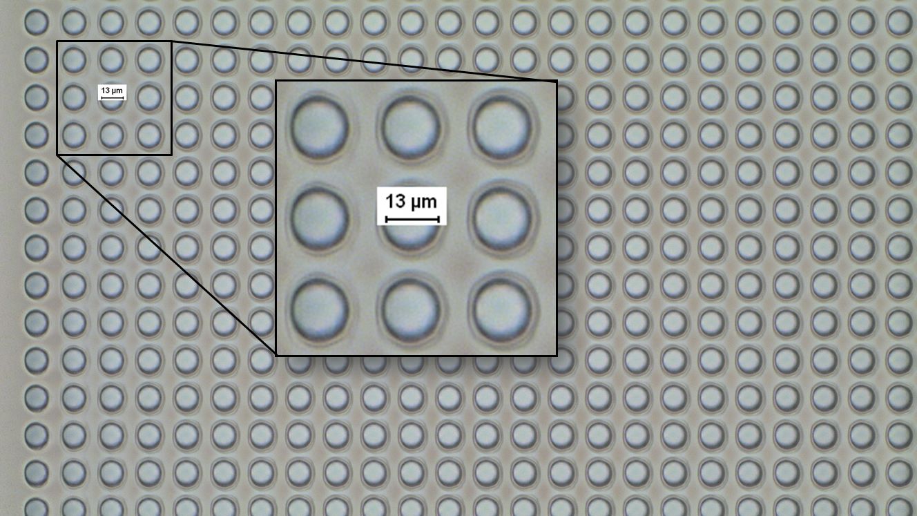
The following images include through vias drilled in 30 µm thin alkali-free glass top view, side view and double-side drilling of a 100 µm thin glass wafer, respectively.