


By Christian Fornaroli
Currently, electrical semiconductor components such as LEDs, solar cells or transistors are commonly produced in a batch process. This way, many identical components can be processed in parallel on one big wafer; subsequently, each chip has to be singulated. Mechanical sawing with diamond blades has been used for a long time, but as the wafer material gets thinner and the chip size smaller, this classical process can be replaced by laser-based dicing processes. In particular, the mechanical load and the relatively large kerf width are serious disadvantages of a mechanical dicing process. A reduction of the kerf width leads to a much higher yield of chips per wafer and, therefore, to increasing efficiency and conserving resources at the same time.
The experiments were carried out with a Coherent HyperRapid 50 at a wavelength of λ = 532 nm, an average power of up to 22 W @ 400 kHz and pulse duration of τ = 6 ps. In this setup, the laser beam is deflected to the workpiece by a Scanlab IntelliScan 14DE Galvo scanner and focused onto a spot diameter of 14 µm by a 100 mm f-Theta lens. The laser source and the entire beam path are installed in a Kugler MICROGANTRY Nano3x with aerodynamic bearings for highest precision. Different fluence levels were investigated as to the cutting depth attainable.
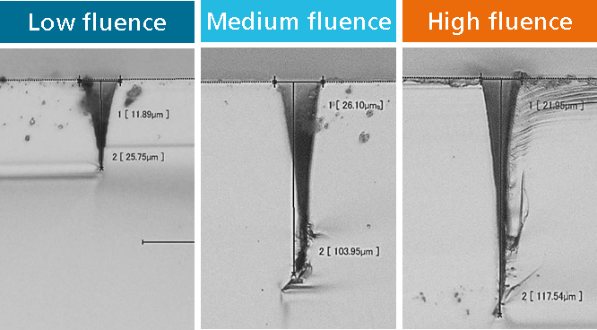
At a pulse repetition frequency of 400 kHz, the scanning speed was set to 2500 mm/s, which means a temporal pulse overlap of 50 percent. Figure 1 shows ablation results for different fluences – 0.75, 5.5 and 10 J/cm² – for up to 1000 repeats. In general it is shown that a sufficient cutting depth of 120 µm cannot be attained with the low and medium fluence. At a fluence of 0.75 J/cm² the cutting depth amounts to almost 20 µm after 400 repetitions and does not rise significantly during the following 600 repetitions. For an increased fluence level of 5.5 J/cm² or pulse energy of 3.1 µJ, the cutting depth after 1000 repetitions is 105 µm.

Although the depth is increased, the progress is again degressive. Even an additional few thousand repetitions will not lead to the desired cutting depth of 120 µm. In contrast, a high fluence level of 10 J/cm² leads to a final groove depth of 135 µm after 1000 passes. The 120 µm are even obtained after 400 repetitions which means an effective cutting speed (scanning speed / number of passes) of 6 mm/s. The groove width also strongly depends on the pulse energy. For low pulse energy, the width amounts to less than 15 µm, or medium and high fluences the groove dimensions increase to 20-25 µm.
Altogether the cutting depth development is logarithmically shaped with different saturation levels, dependent on the fluence level. Once the saturation area is reached, the depth no longer increases significantly. It is likely that the subsequent repetitions even cause damage: cracks and melting zones in the chips. Figure 2 shows light microscope pictures of ablation results for the three different fluence levels. After a particular experiment was conducted, the wafer was cleaved perpendicular to the cutting direction, thus exposing the cutting geometry. The groove shapes at different fluence levels differ only marginally. Big differences occur in terms of the depth attained. At a high fluence, micro cracks can be observed at the cutting edges.
The observed ablation behavior is affected by a multi-pass ablation strategy using a Gaussian beam profile together with the material properties of silicon or semiconductors in general. In a multi-pass ablation strategy, the beam is guided over the workpiece several times. In every repetition a certain amount of material is removed out of the cutting groove. During the first repetition, the Gaussian beam hits a flat surface perpendicularly. Thus, the complete fluence or intensity of the beam is available for the ablation process. After the first repetition, the irradiated area is no longer planar, and the incoming laser beam is projected to the walls of the cutting kerf. Therefore, the effective beam diameter increases, and the fluence decreases. Figure 3 shows an ablation geometry and the dependency of the projected intensity from the angle of incidence.
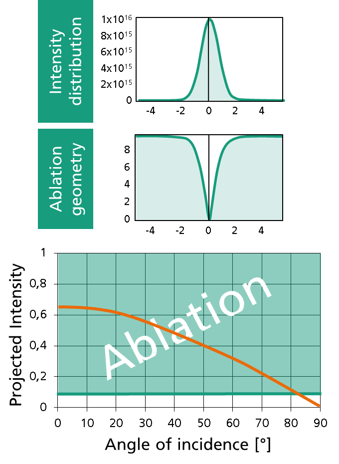
The occurring critical angle determines the attainable cutting depth in relation to the cutting width, and thus explains the observed dependency of the cutting depth on the fluence. Also, the appearance of a saturation level can be explained, because once the critical angle is reached, almost no ablation takes place inside the cutting groove anymore. The steepest point with the critical angle always occurs in the center, due to the highest fluence at this point. However, thermal effects can change the ablation threshold temporarily and multi-reflexes can change the effective angle of incidence. Therefore, the cutting kerf may not develop absolutely vertically, but can drift to one side (compare Figure 2, middle image).
In conclusion, dicing thin silicon wafers with an ultra-short pulsed laser system has been investigated as to which cutting depths and kerf widths can be reached. According to the experiments, the amount of the groove depth strongly depends on the laser fluence. The depth of the kerf develops logarithmically with a saturation level after a certain depth or number of passes. Afterwards the depth no longer increases. This correlation is the result of a multi-pass ablation strategy with ultra-short pulsed laser radiation, in which a critical angle of incidence limits the attainable cutting geometry and depth.
Christian Fornaroli is a research engineer with Fraunhofer ILT.